


Patent Prosecution/ Utility model Prosecution/Industrial Designs/ Trademark/ Litigation/Opinions & Counseling
<< §1 << §2 §3
§3 The Third Industrial Revolution Occurred in Sendai:
In the international conference called the "Berlin Energy Transition Dialogue 2015” which was held in March 2015, it is reported that a huge applause from the participants of various countries were sent to Rifkin’s "The Transition to Zero Marginal Cost Renewable in Energy and the Third Industrial Revolution" presentation.
The European Union has already adopted Rifkin’s "Economic Action Plan of the Third Industrial Revolution," and Rifkin proposes to say that “Internet technology and renewable energies were about to merge to create a powerful new infrastructure for a Third Industrial Revolution (TIR) that would change the world”.
A little different to Rifkin’s theory, but in this column, we state the era of internet technology having the basic optical communications technology since 1950 as the "TIR".
From the aspect of the Energy Revolution, the TIR is the Fourth Energy Revolution using optical energy. Also from the aspect of the Communication Revolution, the TIR is the "Third Communication Revolution", pertaining to a two-way communication of digital information via the internet technology based on optical communication..
John Farndon has announced that the reader’s poll results show that the first place of greatest invention of mankind is now the Internet (John Farndon, "The World's Greatest Idea: The Fifty Greatest Ideas That Have Changed Humanity ", Icon Books Ltd, p.310-317, 2011). The fifth place is the “Use of Fire”, by John Farndon.
Prof. Yagi was the mentor who has led the direction of Tohoku-University’s research with guideline words of "Frequency is asset". The third Information Revolution is positioned as the Frequency Revolution which raised the frequency from the region of radio waves of the second Information to the region of light.
As previously mentioned in §1, the hardware elements implementing the basis of the internet technology, or the three essential elements of optical communication, were all invented by Prof. Nishizawa;
the semiconductor laser patent JP 273217B of 1957 being the light source, the graded-index optical fiber patent (JP Application No.1964/64040) of 1964 as the transmission line and the pin photodiode patent JP 205068B of 1950 as the optical receiver.
This is the reason why Fig. 5 indicates the beginning of the TIR as 1950.
From the 1950’s and 1960’s, the spreading of commercial computers started, and in the 1970’s, computers became in use in the field of manufacturing products, but this is greatly due to the low cost of network connection of computers by optical communication technology.
JP 487916B and US Patent No. 4629901 pertaining to a photo-coupler, which enable impedance conversion by changing the phases and ground point in the optical coupling, have become a necessity technology to the electronic circuit implementation. JP 487916B is recognized and registered as one of the basic IC patents by the Japanese Electronic Industry Development Association. Patents of JP 487916B, JP 506805B, JP 511342B, JP 692061B, JP 762975B, JP 830040B, and JP 851876B etc are all inventions of optoelectronic elements, which are not limited to photo-couplers, but have a wide application span.
As a group of patents using the laser diode which implements the basis of optical logic circuits or optical computers, US Patent No. 3760201 and 4603420, JP 772199B, JP 781848B, JP 812534B, JP 852321B, JP 867834B, JP 896516B, JP 1083895B, JP 1105303B and JP 1207725B have been registered. There are other patents pertaining to optical amplifiers, information recording and arithmetic logical operation such as JP 921469B, JP961569B, JP 992080B, JP 992081B, JP 1083902B and JP 143759B5.
Patent (JP954040)pertaining to a high speed optical modulation by external irradiation of laser light, which implements a basic technology of optical computer, patents(JP521361,JP575455,JP772879,JP830041,JP838678,JP874279,
JP992088,JP1083859,JP164848,JP1418108)pertaining to an optical control, and patent(JP852683)pertaining to wavelength conversion, which implement basic technologies for realizing optical ICs and optical computer architectures, are also proposed.
As already explained, although Tesla's patent (US Patent No. 645,576) pertains to the invention of electric power transmission, the court had made the decision that the Marconi patent was invalid, because US Patent No. 645,576 discloses that Tesla had already recognized that it was possible to use a transmitter and a receiver in wireless communications. The court decision means that photoelectric conversion technique used in optical communication could be used in the field of energy.
Namely, the technology of the pin photo diode as the receiver could be used as the source of electrical energy as a solar cell, and the technology of the semiconductor laser could be used as the source of optical energy in illumination as light emitting diodes (LED).
The light source in the Paris Exposition Universelle of 1900, which was held under the theme of "light and energy", was the incandescent lamp, emitting electrical energy by a high temperature light source. In the TIR, optical energy is emitted from the semiconductor element which is a low temperature light source. Namely, electrical energy is converted directly into optical energy in the TIR.
The LED is the simplified structure of the semiconductor laser, and in terms of generating light using a p-n junction in a semiconductor crystal, the semiconductor laser and the LED are in principle, the same semiconductor light emitting elements. Not only semiconductor lasers but LEDs could also be used for optical communications, and in 1966, a patent application was filed for high frequency operating LED for optical communications, and achieved the patent as JP 609923B.
Visible LED by the p-n junction is already achieved in 1962 by Nick Holonyak and S. F. Bevacqua of GE Company, but it was very dark with electricity-to-light conversion efficiency with less than 0.1% (Nick Holonyak, SF, Bevacqua, "Coherent (visible) Light Emission from Ga (As1-xPx) Junctions", Applied Physics Letters, 1, pp82-83,1962).
To generate light from a semiconductor crystal with a p-n junction, the perfectness of the semiconductor crystal is important, and Prof. Nishizawa’s research on the perfectness of crystal quality begin around 1950, by examining the composition of pyrites (FeS2).
The composition ratio of pyrites should be sulfur (S) 2 to iron (Fe) 1, but in reality, S varies from the range of 2.03 to 1.94 against Fe 1, and Prof. Nishizawa had confirmed through the experiments that electrical characteristics also change (Watanabe, Nishizawa and Sunagawa, “As to geology-thermometer using pyrites”, Science (KAGAKU in Japanese), vol.21, No.3, Iwanami-shoten, p140-141, (1951)). That is, if S is 2 to Fe 1, the stoichiometric composition (stoichiometry) is achieved. And if S is in the range of 2.03 to 1.94 to Fe 1, it means that it is out of the range of stoichiometry.
[Fig. 8]
In the case of gallium phosphide (GaP), it must be phosphor (P) 1 to gallium (Ga) 1, but when measured precisely, in reality it is out of the range of the ratio 1:1, and out of the range of stoichiometry. Prof. Nishizawa proposed a unique crystal growth method called the liquid phase epitaxy (LPE) by a temperature difference method (TDM) under controlled vapor pressure which enabled to grow stoichiometrically controlled III-V compound semiconductor perfect crystals.
"LPE by TDM under Controlled Vapor Pressure (TDM-CVP)” is a method when the high temperature liquid (liquid phase), which is the dissolved material of crystal growth is in contact with the low temperature semiconductor substrate with arranged temperature difference, and when the other element of the compound semiconductor is vapor pressured, the other element dissolves more than the saturation solubility, and it enables to increase the content of the other element and control the ratio (stoichiometry) of the element from another element composing the semiconductor compound grown on the semiconductor substrate.
For example, it is a method when the high temperature liquid (liquid phase) of gallium (Ga) and phosphor (P) dissolved material for the crystal growth is in contact with the gallium phosphide (GaP) semiconductor substrate with predetermined temperature difference, and when P is vapor pressured to the high temperature liquid, the P density diffuses along the temperature gradient and dissolves more into the high temperature liquid than the saturation solubility.
Because P can be dissolved more than the saturation solubility, the control of stoichiometry is possible by increasing the content of P, which will build up the to-be-grown GaP crystal, and according to "LPE by TDM-CVP”, Prof. Nishizawa experimentally showed that the ratio of Ga and P has been controlled precisely to 1:1.
Many academic researchers and scholars considered, at that time, that Nishizawa’s method was contradicting to the equilibrium law of the solid-liquid-gas phase by the US theorist Josiah Willard Gibbs. That is, according to Gibbs’ equilibrium law, saturation solubility at a certain temperature should be constant. In Gibbs’ equilibrium law, it meant that it was not possible to dissolve P more than saturation solubility, and therefore, strong oppositions came from the Association for Crystal Growth. Then, Nishizawa’s LPE method has a history that submitted papers by Prof. Nishizawa being continually rejected at peer reviews stages.
At that time, it was said that no light will be emitted unless nitrogen was doped as an impurity to the gallium phosphide (GaP) based crystals. Rejected as the violation to Gibbs’ equilibrium law, by the LPE by TDM-CVP, the patent application for the crystal growth method of controlling the ratio of Ga and P within GaP of GaP precisely to 1:1 was filed in 1975 and was patented as JP 1038323B.
By controlling the stoichiometry of GaP, Prof. Nishizawa confirmed that the pure green light emission can be obtained from the crystals without the doping of nitrogen, and patent applications were filed in 1979 and 1980, patented as JP 1516291B and JP 1437621B respectively. And, the technology being transferred and manufactured by Stanley Electric Co., Ltd., the pure green LED by GaP based crystals showed the highest efficiency and brightness in the world by the scheme of "LPE by TDM-CVP”.
Also, with respect to the red LED of gallium-aluminum-arsenide (GaAlAs) based crystals, patent applications filed in 1976 achieved the patents as JP 1018805B, JP. 10250238B, JP 1270761B, and patent application filed in 1980 achieved a patent as JP 1264270B etc, as LPE by TDM-CVP patents. These technologies of growing crystals by controlling stoichiometry by “LPE by TDM-CVP” for GaAlAs based crystals were also transferred to and produced by Stanley Electric Co., Ltd. and continued to update the top data of LEDs for the highest efficiency and brightness in the world.
In fact, when considering the equilibrium of solid-liquid-gas phase, and taking in mind of the stoichiometry deviation of the crystal organizing the solid phase, in terms of chemical energy, the phenomenon of the other element building up the crystal dissolving more than saturation solubility does not violate Gibbs’ equilibrium law, but it took a long time of 18 years to be understood.
In the international conference held in Toyohashi in 1971, Prof. Nishizawa announced the experiment results of LPE by TDM-CVP and received strong oppositions. After 18 years had passed in 1989, finally the International Organization for Crystal Growth (IOCG) acknowledges LPE by TDM-CVP. Prof. Nishizawa became the first winner of the Laudise Prize founded in 1989. The Laudise Prize is a prize which is awarded once every three years, and is presented for significant technological (not necessarily experimental) contributions to the field of crystal growth.
Furthermore, an invention of controlling the stoichiometry by applying high vapor pressure, which is not limited to the LPE by TDM-CVP and can be applied to growth of II-VI compound semiconductors such as ZnS, CdS, ZnSe and HgTe, was also filed already in 1971, and has been patented as JP 1074051B.
Drs. Akasaki, Amano, and Nakamura were awarded the Nobel Prize in Physics in 2014, after Drs. Akasaki and Amano have filed a patent application in 1985 for the blue LED by gallium nitride (GaN) crystals, which has been granted as JP1992-15200B, and registered as JP 1708203B, and after Dr. Nakamura has filed a patent application in 1990 for the blue LED by GaN crystals, which is registered as JP 2628404B.
Contrary to GaN, Prof. Nishizawa had selected zinc selenide (ZnSe) crystal, which is the II-VI compound semiconductor, in order to achieve the blue LED. And, a patent application for the invention of making perfect crystals of ZnSe with “LPE by TDM-CVP” was filed in 1980 and achieved the patent as JP 1362385B, and also patent applications were filed in 1981 and achieved the patents as JP 1345720B and JP 1427448B. The counterpart US patent application of JP 1427448B is issued as US Patent No.4783426.
US Patents of Green LED using ZnSe p-n junction are issued as US Patent No.4725563 and 4755856, which claims benefit of priority under 35 USC 119 based on Japanese Patent Application No. P1982-118037 filed in JPO on July 6, 1982.
Furthermore, Prof. Nishizawa also filed patent applications in 1982 for the II-VI compound semiconductor by “LPE by TDM-CVP”, and achieved the patents as JP 1272449B, JP 1313593B, JP 1317587B, JP 1317589B, JP 1317594B, and JP 1328673B. The counterpart US patent applications of JP 1313593B and JP 1328673B are issued as US Patent No.4917757 and 4968491, respectively.
Using the ZnSe crystal obtained by “LPE by TDM-CVP”, Prof. Nishizawa has achieved the blue LED by emitting blue light from the p-n junction in 1983, dating back two years before than those by Drs. Akasaki and Amano.
The basis of the technical concept of the patent invention of JP 2628404B by Dr. Nakamura is the control of the stoichiometric composition of the GaN crystals. The fact must not be forgotten that Prof. Nishizawa has continued the research on stoichiometric composition of the compound semiconductors for more than 30 years, ever since Prof. Nishizawa disclosed the importance of the control of the stoichiometry of compound semiconductors from the pyrite results in “Science (KAGAKU in Japanese) in 1951.
From the explanations mentioned above, it is understandable that the true contributor for the development of LED lighting is Prof. Nishizawa, and therefore, the fourth Energy Revolution (the TIR) was born in Sendai.
Fig. 9 shows the luminous flux (measured in lumen) per unit electrical input power (measured in watt) in the vertical axis, timeline in the horizontal axis, which is the redraw of Fig. 5.
[Fig. 9]
According to the "Light Bulb Hall of Fame Inventors List” in the "Light Bulb Chronicle" published by GE Company, Edison is the 25th inventor. The first inventor on the list is the British Humphry Davy with the arc lamp of 1809. And the first substantial inventor of the incandescent light bulb with carbon fibers is said to be Sir Joseph Wilson Swan of Britain in 1878. It appears that Edison started to develop the incandescent light bulb a year after Swan’s invention in 1879.
Brief history of the development of the incandescent light bulb, before Thomas Edison began serious research on incandescent lamp in 1879 is as follows:
1802 Humphry Davy invented the first Light Bulb using a platinum strip exposed to air;.
1809 Humphry Davy invented the Electric Arc lamp using carbon electrodes;
1809 (Uncertain) Thomas De la Rue used a platinum coil in a glass tube?;
1820 De la Rue and De la Rive are credited with making a filament incandescent lamp with a coiled platinum wire;
1835 James Bowman Lindsay demonstrated an incandescent light;
1838 patent by J.B.A. Marcellin Jobard;
1839 Marcellin Jobard suggested that mines could be illuminated by running an electric current through a carbon filament in a vacuum;
1841 Frederick de Moleyns got a patent inclosing a platinum wire in a vacuum bulb;
1845 patent by John Wellington Starr with a platinum strip and graphite rod in vacuum (British patent No. 10,919 in the name of Edward Augustin King);
1849 William Petrie used iridium and iridium alloys in the air;
1850 Joseph Wilson Swan enclosed carbonized paper filaments in an evacuated glass bulb;
1851 the magician Jean Eugène Robert-Houdin demonstrated incandescent lights at his estate;
1850 Edward C. Shepard enclosed charcoal cylinder in vacuum;
1854 Heinrich Goebel enclosed carbon filament in vacuum;
1856 Charles de Changy carried a flashlight into the mines consisting of a platinum filament, and got a patent;
1860 patent by Joseph Swan;
1872 Alexander Lodygin invented an incandescent light using carbon rods in a nitrogen-filled bulb;
1874 Henry Woodward and Mathew Evans enclosed carbon rods in glass cylinders filled with nitrogen(Canadian patent No.3,738);
1878 Swan developed a longer lasting light bulb;
1878 Patent by H. Woodward(U.S. Patent No. 181,613);
1878 Patent by William Sawyer (U.S. Patent No. 194563);
1878 Patent by William Sawyer and Albon Man(U.S. Patent No. 205144)
Taking into account of the fact that Antonio Meucci invented the telephone around 1854, Fig. 5 shows the beginning of the second Industrial Revolution (SIR) as 1860, but in reality, including the time period of light bulb invention, there is a range regarding the beginning of the SIR, so the scale of the horizontal axis in Fig. 9 is not clear.
In terms of the TIR as the revolution which uses optical energy, Prof. Nishizawa proposed crystal growth using optical energy in 1961 (Jun-ichi Nishizawa, "Molectronics (I)", The Japan Institute of Metals and Materials Journal, Vol. 25, No. 5, pA149-A157 (1961)). Then, it is reported that the optically excited crystal growth method for silicon (Si) using optical energy was first achieved in the world in 1963 (Jun-ichi Nishizawa et al, “The Influence of Ray of Light to Gas-Phase Growth”, General Research, Document No. 37-19, p1-5, (1963)).
There is a dark region in the development of frequency from the SIR to the TIR, and the optical region was used in the industry first and afterwards, the frequency region between the radio waves and light was developed in the TIR. This dark region is known as the terahertz waves region, anciently called the far-infrared rays or the sub-millimeter waves.
In 1963, Prof. Nishizawa proposed that the lattice vibration within the semiconductor is a promising candidate as a source of electromagnetic waves in this dark area (Junichi Nishizawa, Electronic Science (DENSHI-KAGAKU in Japanese), Vol. 13, No. 4, p17, (1963)), and in 1972, the patent applications pertaining to a signal amplifier oscillation element and a signal conversion amplifier oscillation element by the Raman effect were filed (JP 840056B, JP 844479B). In 1972, the Raman laser patent application has been filed (JP 1392926B).
And in 1980, a report was released that an electromagnetic wave at 12THz frequency was successfully oscillated from the lattice vibration of GaP crystals in Raman laser (J. Nishizawa et al, "Semiconductor Raman Laser", J. Applied Phys., Vol . 51, p2429 (1980).
Currently, Prof. Nishizawa has achieved several patents as shown in Fig. 10, including frequency variable lasers between 0.5 THz ~ 7 THz, covering electromagnetic waves over 3 THz. The counterpart US patent application of JP 139296, 1431581, 1431582 is issued as US Patent No.4571727. Furthermore, the counterpart US patent applications of JP 4272111B and JP4749156B are issued as US Patent No.7912553 and 7599407, respectively.
And some of the patents in the group shown in Fig. 10 have been technology transferred to Terahertz Laboratory Co., Ltd. in Akita Prefecture, and products are commercially available.
[Fig. 10]
The challenge to the higher-frequency operation from the radio wave side of the electromagnetic wave to the terahertz wave region was also continued by Prof. Nishizawa. Namely, as a terahertz wave band transistor, Prof. Nishizawa has achieved the patents for the so-called mesoscopic SITs with atomic order scale, or the ideal SITs (JP 1511551B, JP 1550798B). The counterpart US patent application of JP 1550798B is issued as US Patent No.4482910. Some mesoscopic SITs are the semiconductor devices using the tunneling effect (JP 1462301B, JP 1482766B, JP 1560100B), and the counterpart US patent application of JP 1560100B is issued as US Patent No.4799090 and 4876580.
The terahertz wave band SIT has been developed and called as “the permeable base transistor” by the MIT in USA, and “the ballistic transistor” by Cornell University, but these are semiconductor elements designed by the theory of quantum mechanics.
The patents have also been achieved for tunnel injection transit time negative resistance (TUNNETT) diodes which are oscillators using the most promising tunneling effect from the range of 100GHz and 1000GHz (JP 12611B, JP 661298B, JP1310746B). The counterpart US patent application of JP 661298B is issued as US Patent No.3602840.
Although the stoichiometry control of the compound semiconductor pertains to a control scheme of molecular numbers, a growing scheme of the semiconductor crystal in units of one molecular layer, by controlling the thickness of a single molecular level is “the molecular layer epitaxy (MLE)”. By the scheme of MLE, it becomes possible to produce microstructure semiconductor elements designed by the theory of quantum mechanics described above.
[Fig. 11]
JP 2628404B which Dr. Nakamura filed in 1990 was a vapor-phase growth method using MOCVD reactor, in which reactant gas, containing the component elements of GaN, and carrier gas are introduced horizontally, while subflow of additional inert gas is introduced vertically from above the semiconductor substrate so as to suppress the deviation of nitrogen atoms from a growth layer, thereby controlling the stoichiometry of GaN in the growth layer.
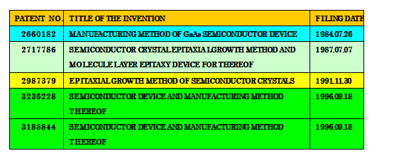
On the other hand, JP 2660182B which was filed in 1984 by Prof. Nishizawa, six years earlier than the patent application by Dr. Nakamra, was a method to grow compound semiconductor one molecular layer by one molecular layer in a ultra-high vacuum reactor, through supplying the component elements of the compound semiconductor from two different directions above the semiconductor substrate, alternately as a pulse to the surface of the semiconductor substrate, thereby controlling the stoichiometry of compound semiconductor.
PUBLISHED WORKS
Patent Claim Drafting under regime of Common Application Format (CAF) agreed by the Trilateral Offices (JPO, USPTO and EPO)
 Essentials of Drafting Patent Specification under regime of CAF agreed by JPO, USPTO, EPO, SIPO and KIPO