


Patent Prosecution/ Utility model Prosecution/Industrial Designs/ Trademark/ Litigation/Opinions & Counseling
OUR BACKGROUND THANKS TO IP SHOGUN NISHIZAWA
IP Shogun Jun-ichi NISHIZAWA:
Prof. Nishizawa was born in 1926, Sendai Japan.
He
received Japan Academy Prize in 1974, the International
Organization of Crystal Growth (IOCG) Laudise Prize in
1989, the Order of Cultural Merits (Bunka-Kunsho)
conferred from Japanese Emperor in 1989. In 2002
“Jun-ichi Nishizawa Medal” was founded in IEEE, U.S.A.
§1 §2 >> §3 >>
§1 Semiconductor Research Foundation based on Patent Income :
The Stanford Research Institute, which was more or less founded for the development and public interest of scientific knowledge rather than for University students, was established mainly by Prof. Frederick Terman, the Dean of the School of Engineering, Stanford University in 1946, at Silicon Valley, United States of America.
In 1938, before the establishment of the Stanford Research Institute, Hewlett-Packard Company had already been founded in Silicon Valley, with Prof. Terman as their mentor. And in 1955, Shockley Semiconductor Laboratory had been founded in Silicon Valley.
Jointly invented by Prof. Watanabe and Prof. Nishizawa, the patents of “pin diode” (JP1953-6077A: JP 205068B) filed in 1950, the “pin photo-diode” (JP1955-8969A: JP 221218B ) filed in 1952, and the” Semiconductor Laser” (JP1960-13787A: JP 273217B) filed in 1957 were very important inventions which became the basis of the semiconductor industry, or Japan’s new industry. And, based upon these donated patents from Prof. Watanabe and Prof. Nishizawa, leaded by Prof. Watanabe as Chairman, the Semiconductor Research Foundation was established.
[Fig. 1]
1946 “Stanford Research Institute” was established in Silicon Valley in USA.
1950 Patent application of pin diode, pnip bipolar transistor (JP 205068B) was filed in JPO 18 days earlier than GE Company, USA;
1950 Patent application of Ion Implantation Method (JP 229685B) was filed in JPO;
1952 Patent application of pin photo-diode (JP 221218B) was filed in JPO; and
1957 Patent application of Semiconductor Laser (JP 273217B) was filed in JPO.
1961 Non-profit organization “Semiconductor Research Foundation” was established, which is independently financed and managed from Tohoku University,
1963 Construction of the Laboratory building of Semiconductor Research Institute of the Semiconductor Research Foundation.
2008 Dissolution of Foundation: Semiconductor Research Foundation was donated to Tohoku University. The ground site, laboratory building and experimental facilities of the Foundation, which are valued as 2.4 billion yen, are currently opened to the public as “Jun-ichi Nishizawa Commemoration Center” in Tohoku University.
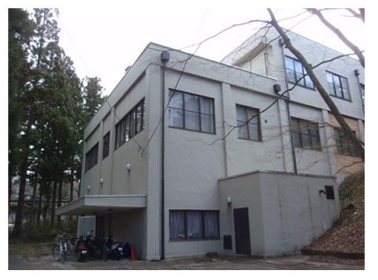
The above mentioned Stanford Research Institute is said to be the model case of the “Semiconductor Research Institute” of the Semiconductor Research Foundation. In 1963, Kawauchi, Aoba-ku, Sendai, the first laboratory building (Laboratory Building No. 1) for “Semiconductor Research Institute” was built, and full-time research staffs, research assistants, experiment assistants and administration staffs were set, having Prof. Jun-ichi Nishizawa as the chief research staff himself.
[Fig. 2] Laboratory Building No. 1 of Semiconductor Research Institute
(Photo as of January 2016)
The Semiconductor Research Foundation, being established by the donated patents from Prof. Watanabe and Prof. Nishizawa, was run with the new patent license incomes produced from the research results according to Prof. Nishizawa’s supervision, and incomes for technical advice for know-hows etc, and these were the financial resources for all of the accounting and management of the foundation, including the manning fees for the research and administration staffs, making it a very unique non-profit foundation.
At that time the establishment of 1961, the term "industry-university cooperation" was not being used, but was called as "industry-university collaboration”. This foundation was the basis of “industry-university collaboration”, bridging the divide between university research and the industrial world. As an organization, financial statements were completely independent from Tohoku University, and it was a foundation required for the capability to "manage research", so there was an expected task to create a new industry come to life with the original research results by Prof. Nishizawa.
As illustrated in Fig. 1, just 18 days earlier than R. N. Hall, GE Corporation, USA, the patent application of “pin diode” was filed in JPO. The patent of “pin diode” was directed not only to a technology for optical communication receivers, but also to a pioneer technology which became the basis for various electronic devices. For this reason, in the early days of the Japanese semiconductor industry which was dependent on the inventions from United States, this patent functioned to prevent the outflow of the Japanese Yen from Japan to abroad. Therefore the invention of “pin diode” largely contributed to the Japanese industry. The refusal of the contract between GE in 1955 by the Japanese Foreign Currency Review Committee was based on this important invention.
Ion implantation method was an essential process for the production of the current miniaturized semiconductor integrated circuit, which was also an invention by Prof. Nishizawa (JP 229685B).
JP 205068B is construed to be a patent including the technical scope of “pnip bipolar transistor”. Although almost 80 percent of the manufactured product of the high-frequency bipolar transistors has infringed the patent claims of JP 205068B, at the time, only Hewlett-Packard Company has payed license fee, responding for the exploitation contract with this patent. There was no compensation toward JP 205068B from the Japanese industry.
The CEO of Hewlett-Packard from 1978 to 1992 is John Young, famous as in Young's Report, submitted in 1985. Hewlett-Packard Company still has its headquarters in Silicon Valley today. The Young Report had given the opportunity to the second pro-patent policy in 1985 by President Reagan, and the pro-patent policy showed global expansion.
Afterwards, disputes over the patent royalties of JP 205068B went on with twists and turns, and Semiconductor Research Foundation was forced to know the difficulty of "managing research." As a final result, the Japanese major semiconductor companies settled to pay two billion Japanese Yen to the Semiconductor Research Foundation. The two billion Japanese Yen were set aside for the purchase of site grounds and constructions for the Laboratory Building No. 2 of the Semiconductor Research Institute of the Semiconductor Research Foundation.
Considering the scale of Japan's semiconductor industry, two billion Japanese Yen was such a small amount. If it was the case for the Nobel Prize awarded in 2015 for Physiology or Medicine to Prof. Satoshi Omura (Advisor of the Kitasato Institute and Distinguished Emeritus Prof. of Kitasato University), he was said to be rewarded 25 billion Japanese Yen from Merck & Co., Inc., USA, and the Semiconductor Research Foundation could have been rewarded much more for the expensive patent license incomes.
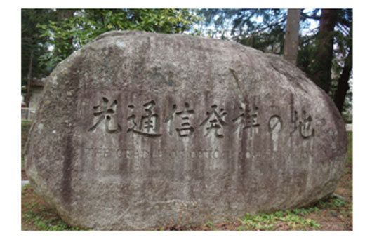
The internet could not be explained without the development of optical communication. The three essential elements of optical communication are the light source, transmission line and optical receiver and these ideas all came from Japan and this is the origin (JP 205068B, JP 273217B, JP1971-29291A). Moreover, the ideas of the three essential elements were all proposed by the same inventor, and these ideas had been donated to the Semiconductor Research Foundation.
Dr. Charles Kuen Kao of STL, UK, who was awarded the Nobel Prize in physics in 2009, is said to have questioned Prof. Nishizawa himself directly, saying ’You have invented the three essential elements for optical communication, the semiconductor laser, the optical fiber, the pin photo-diode, and yet why do not the Japanese people call you as the “Father of Optical Communication” ?’
[Fig. 3] The stone monument of the "Birthplace of Optical Communication" on the site grounds of the Laboratory Building No. 1 of the Semiconductor Research Institute.
 The patent application (JP Application No.1964/64040) for graded-index optical fiber was granted for a patent and was published as JP1971-29291(B4), but was widely criticized from the Japanese industry after the publication. And in the proceedings of the patent opposition procedures after the publication of the examined application, the examined application has not been registered as a patent, according to the judgment that it has not met the “Requirements of a Divisional Application" (Sohbe Suzuki “Comments on the Requirement for Divisional Application--Why the Patent Application of the Optical Fiber has been rejected?", Intellectual Property Management, Vol. 51, No. 1 pp.27-40, 2001.).
“Requirements of a Divisional Application" has been subsequently revised. According to the current patent law, the optical fiber patent should have been recognized as an important patent in history. It should be said that there was a defect in the patent law at the time. In order to manage a research, it is necessary to review the support system and support from the industry.
The history of optical fiber is long, and Prof. Nishizawa is not the only one who invented all the structure of the optical fiber. Already in October 1926, John Logie Baird from the United Kingdom filed a patent application with hollow pipes and glass-plastic rods in a bundle as an optical conduction path, and has been granted as a patent in 1928 (British Patent No. 285,738). Yet, Baird is known to be the as the developer of mechanical television system using a Nipkow disc, and in January 1926, he was successful in sending and receiving moving silhouette images in a public experiment at the Royal Institution in London.
Shortly later, Clarence W. Hansell of RCA, USA filed a patent application with the idea to send an optical signal for a facsimile by glass fibers and this was granted as a patent in 1930 (US Patent No. 1,751,584). Both British Patent No. 285,738 and US Patent No. 1,751,584 were optical fibers without clads.
And in 1960, Elias Snitzer of American Optical Corporation proposed a structure composed of a single-mode type optical fiber with clads (US Patent No. 3,157,726; E. Snitzer, "Cylindrical Dielectric Waveguide Modes", J. Opt. Soc. Am. Vol 51, p491 (1961)).
In comparison with the single-mode type, the invention by Prof. Nishizawa was a multi-mode type. It was a graded-index optical fiber which enabled to gather the ray of light with different angles of incidence by continuously decreased parabolic refractive index of the core glass fiber from the core towards the periphery.
The thesis of 1966 by Dr. Kao of STL showed that it was possible to reduce the loss of light by lowering the impurity concentration of glass (CK Kao et al. Proc. Inst. Elec. Eng., Vol. 113, no.7, pp.1151-1158, July (1966)).
In autumn of 1965, during the presentation of the graded-index optical fiber at the Institute of Electronics, Information and Communication Engineers (IEICE), one of the researchers of a certain institute removed his glasses from the face and exclaimed quite sharply that, “Even with this thickness of 1mm lens, it gets darkened. You will see nothing, blackened with the thickness of 30 cm glass. Moreover, light will never reach the other end for tens of kilometers. How on earth could you suggest communicating through those?” Of course, the presentation hall roared with laughter (Jun-ichi Nishizawa, "Originality is within the Battle", pp. P155, President, Inc., 1986).
Although N. G. Basov of the Lebedev Institute of the former Soviet Union has proposed his paper --the technical level was rather inferior-- two years after Prof. Nishizawa’s patent application of semiconductor laser in 1957, N. G. Basov was awarded the Nobel Prize in physics for the same research 1n 1964, with C. H. Townes and A. M. Prokhorov for " inventions of maser, laser and fundamental work in the field of quantum electronics".
Laser patents are obtained by Townes (Arthur L. Schawlow, and Charles H. Townes, US Patent. No. 2,929,222). However, Gordon Gould who was 37 years old, a student of the Columbia University had invented a device to produce a light stimulated emission in November 1957, and named this light as LASER (Light Amplification by Stimulated Emission of Radiation), as records show rough calculations and the word LASER in his laboratory notebook.
After the 20 years court fight between Gould and Townes, the patent was granted for Gould and it is said in the United States that the true inventor of laser is to be Gould. However, the filing date of the JP 273217B is April 1957, and is seven months earlier than the date of Gould’s study notes. Prof. Nishizawa is the true inventor of “LASER”, rather than the inventor of "semiconductor laser”.
[Fig. 4]
Apr 1957 Filing of patent application for Semiconductor Laser by Watanabe & Nishizawa.
Nov 1957 G. Gould invented a light stimulated emission device and named this light LASER (Light Amplification by Stimulated Emission of Radiation), and recorded the idea with rough calculations in his laboratory notebook.
Jul 1958 Filing of patent application for Laser by A. L. Schawlow and C H. Townes.
Apr 1959 Filing of patent application for Laser by G. Gould
Mar 1960 Laser Patent by A. L. Schawlow and C H. Townes issued (US Patent No. 2,929,222).
Jun 1960 Experimental success of ruby laser pulse oscillation by T. H. Maiman.
1961 Thesis on Semiconductor Laser by N. G. Basov.
1964 C. H. Townes and A. M. Prokhorov awarded for Nobel Prize in physics.
Nov 1987 Laser Patent by G. Gould issued (US Patent No. 4,704,583).
Progress in research areas of semiconductor device is rapid, and most of the semiconductor manufacturing apparatus needs billions of expense. Under the doctrine of Prof. Nishizawa such that “For achieving original research-work, we must build research-instruments by ourselves”, research staffs of the Semiconductor Research Foundation are always self-building most of the semiconductor research facilities by themselves, but the self-building scheme is was also for reducing the research cost fees.
For example, most of all of the research staffs, research assistants, and experiment assistants of the Semiconductor Research Foundation had the technology to wind the electric furnace. It is said that the invention being awarded for Nobel Prize in physics in 2014 for Prof. Akasaki and Prof. Amano accorded to the malfunction of the electric furnace. If it was the case of Semiconductor Research Foundation, discoveries as such as Prof. Akasaki’s and Prof. Amano’s would have never happened. This was because malfunction of the electric furnace would have been immediately repaired by the experiment staff himself.
Unfortunately, the Semiconductor Research Foundation dissolved on March 31, 2008. Donated to the Tohoku University, the site grounds, research buildings (Laboratory Building No. 2 and Laboratory Building No. 3) and facilities (Valued as 2.4 billion yen) of the Semiconductor Research Foundation are currently opened to the public as “Jun-ichi Nishizawa Commemoration Center”. Laboratory Building No. 1 of the Semiconductor Research Institute is now "Nishizawa Commemoration Library" in Tohoku University, which remains within the Kawauchi campus of Tohoku University.
PUBLISHED WORKS
Patent Claim Drafting under regime of Common Application Format (CAF) agreed by the Trilateral Offices (JPO, USPTO and EPO)
 Essentials of Drafting Patent Specification under regime of CAF agreed by JPO, USPTO, EPO, SIPO and KIPO